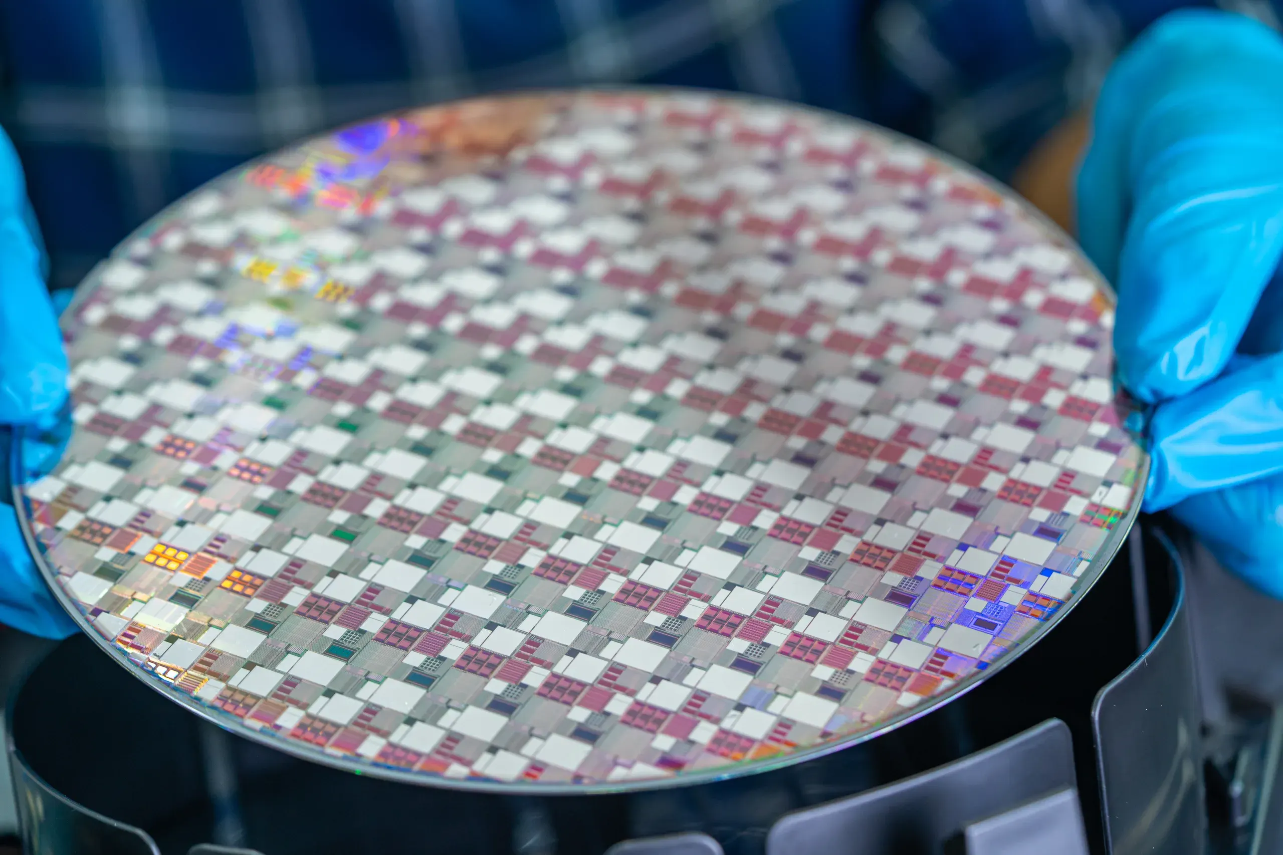
Specialty semiconductor equipment & process services
Etch, deposition and thermal processing — matched to your process
RayFan Semi is an independent equipment and process-solutions company headquartered in Hsinchu, Taiwan. We help MEMS, power, compound-semiconductor and advanced-packaging teams specify, evaluate and support production-proven process equipment from established international manufacturers.
What we do
Three connected lines of business
Equipment only creates value when the process, the installation and the long-term support all hold together. We are built around that whole chain, not a single transaction.
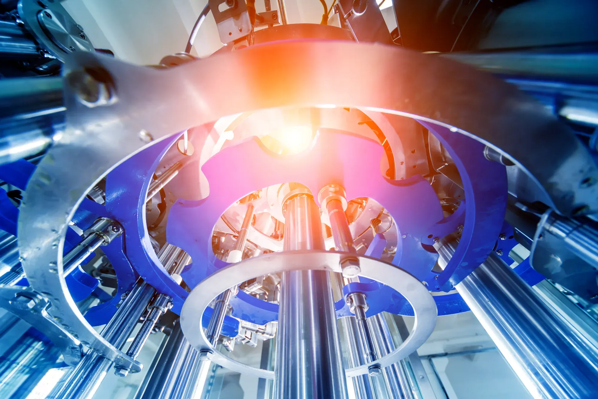
Plasma process equipment
Deep silicon etch (DRIE), reactive ion etch, vapor-phase HF sacrificial release and PECVD dielectric deposition platforms for MEMS, power and compound-semiconductor manufacturing.
- High-aspect-ratio silicon structures
- Low-damage compound-semiconductor etch
- Low-stress dielectric films
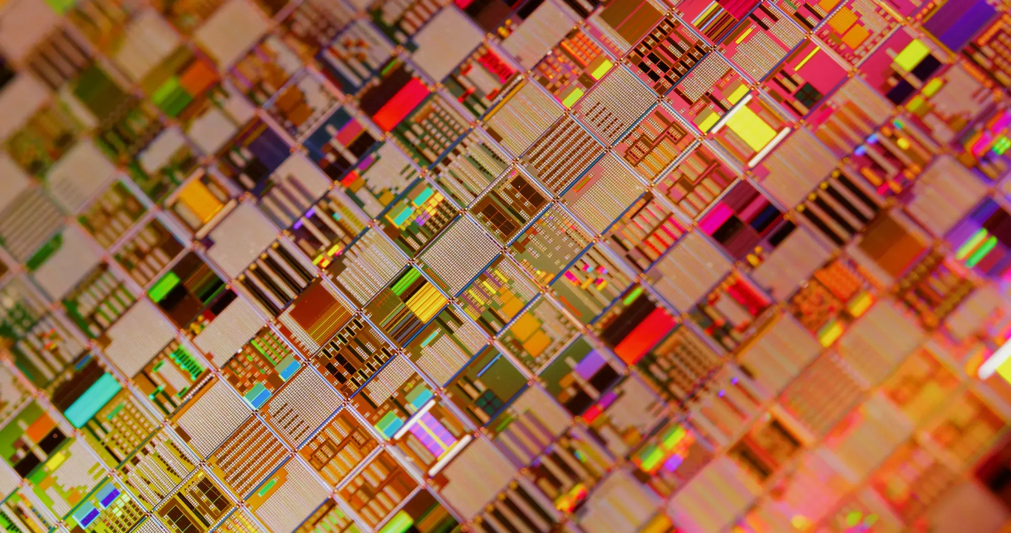
Thermal processing
Batch furnace systems for oxidation, diffusion, annealing, LPCVD and APCVD — the thermal backbone of power-device, sensor and specialty-CMOS process flows.
- Vertical and horizontal batch furnaces
- Oxidation, diffusion and anneal
- LPCVD / APCVD film growth
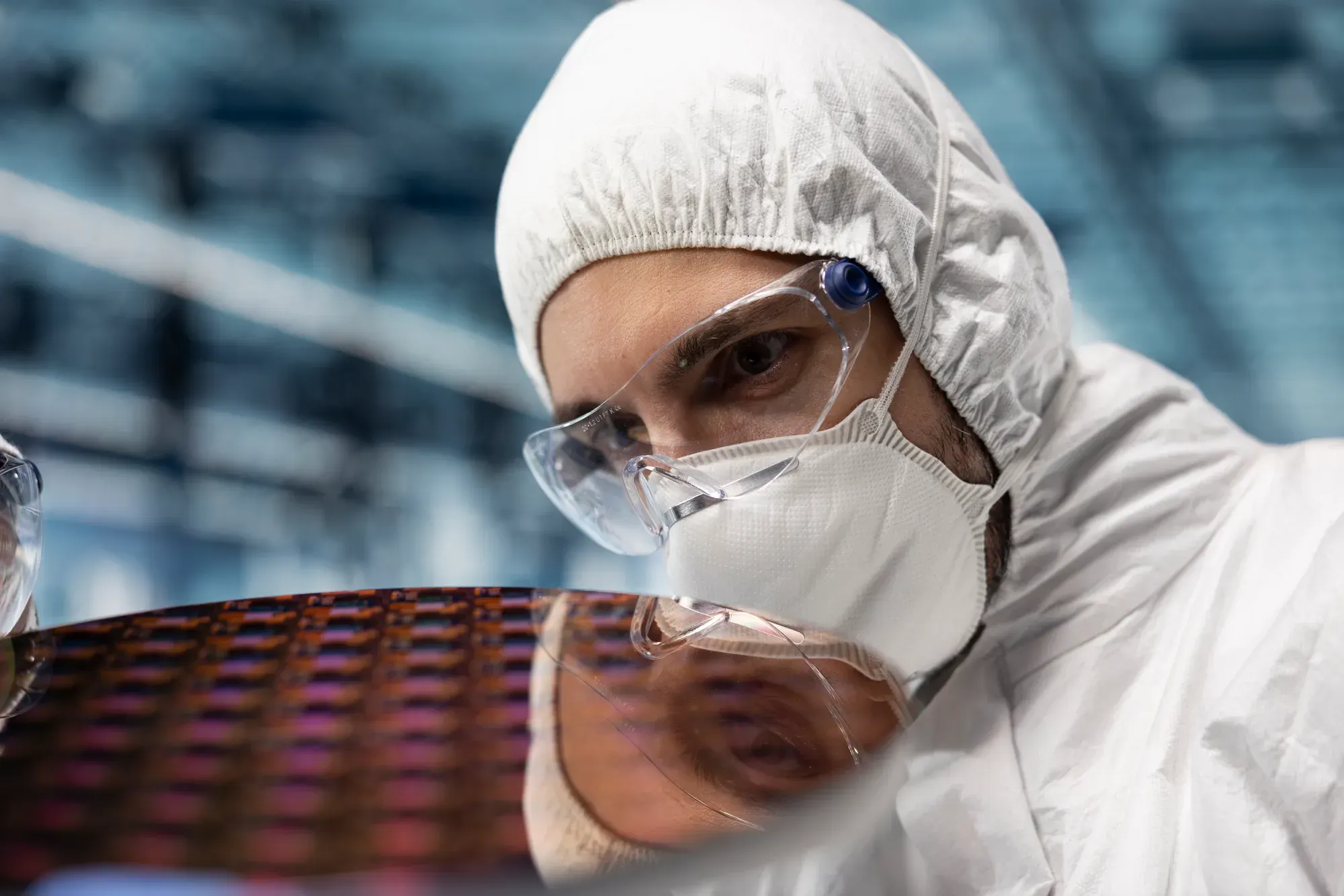
Process & field services
Application assessment, demo and sample coordination, installation readiness, and long-term service and parts coordination — delivered in your language and your time zone.
- Application & feasibility assessment
- Demo definition and coordination
- Installation and lifecycle support
Who we serve
Built for specialty semiconductor manufacturing
Every engagement starts from your device and your process window — not from a product catalogue.
MEMS & sensors
Deep silicon structures, SOI devices, sacrificial release and low-stress films for inertial, acoustic, pressure and optical MEMS.
Explore this field02SiC & GaN power
Trench etch, low-damage processes and passivation films for silicon carbide and gallium nitride power devices.
Explore this field03RF & photonics
Precision etch and dielectric deposition for filters, waveguides, laser facets and integrated photonics.
Explore this field04Advanced packaging
TSV silicon etch and low-temperature dielectric deposition steps for 2.5D/3D integration and wafer-level packaging.
Explore this field05R&D & pilot lines
Flexible configurations for universities, institutes and pilot production — with a path from lab to fab.
Explore this fieldHow we work
A transparent path from first question to supported tool
High-value equipment decisions deserve a process you can audit. Ours has six stages, and every stage produces something you keep.
Application review
We start from your structure, materials, wafer size and acceptance criteria — under NDA where needed.
Feasibility with the manufacturer
Your requirement is translated into a concrete platform and configuration question, answered by the manufacturer’s process engineers.
Demo & sample evaluation
Success metrics are agreed in writing before any wafer is processed. You judge results against your own criteria.
Configuration & terms
Final configuration, facility requirements, documentation and commercial terms are settled in parallel — no surprises late in the project.
Delivery & installation
Factory acceptance, shipment, site preparation and installation are coordinated against a documented checklist.
Lifecycle support
Training, maintenance, parts and process questions are handled long after sign-off. Equipment is a relationship, not a shipment.
Why RayFan
An engineering partner, not a trading desk
The equipment market has enough intermediaries. What specialty fabs lack is a counterpart who speaks process, takes responsibility for the details and stays after the invoice.
Application-first engagement
Discussions start with etch profiles, film stress and throughput — not with a price list. If a platform is not the right fit, we say so.
One counterpart, end to end
Specification, demo logistics, documentation, shipping and installation are coordinated by one team — you are not assembling a project out of three suppliers and a freight forwarder.
Cross-region coverage
Headquartered in Hsinchu, working in Mandarin and English across Greater China and the wider Asia-Pacific region.
Built for the long term
Our model rewards installed tools that keep running — service, parts and process support are the core of the business, not an afterthought.
Insights
Engineering notes for equipment decisions
12 inputs to define before starting a Si DRIE project
Most DRIE projects that stall share one root cause: the application was never fully defined. Here are the twelve inputs to pin down first.
Read articleHow to define success for a deep silicon etch demo
A single beautiful cross-section photo proves very little. What a meaningful DRIE demo looks like, and the criteria to agree in writing before processing starts.
Read articleVertical vs horizontal batch furnaces: a selection framework for oxidation, diffusion and LPCVD
Batch thermal processing remains the quiet backbone of power and sensor fabs. A framework for the vertical-vs-horizontal decision, and the evaluation data that actually settles it.
Read article
Have a structure, film or thermal step to discuss?
Send a short description of your application — device type, material, wafer size and what a good result looks like. An engineer will reply with a concrete next step.